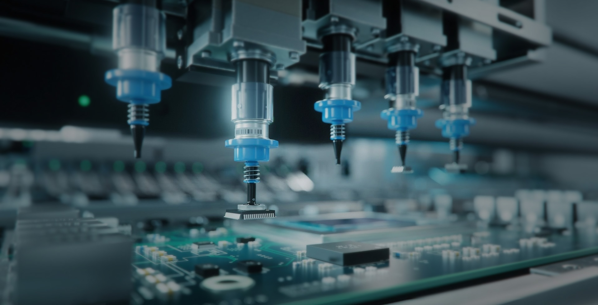
Pushing the physical limit of 0.036mm to set the high-yield metallization standard for 1.6T optical communication and super flagship smartphones.
Board Thickness Range
0.036-2.4mm
Aspect Ratio (AR)
8:1 / 10:1
Replacement Rate
10 TO/hr
Yield
99.8%
Detail Section 01
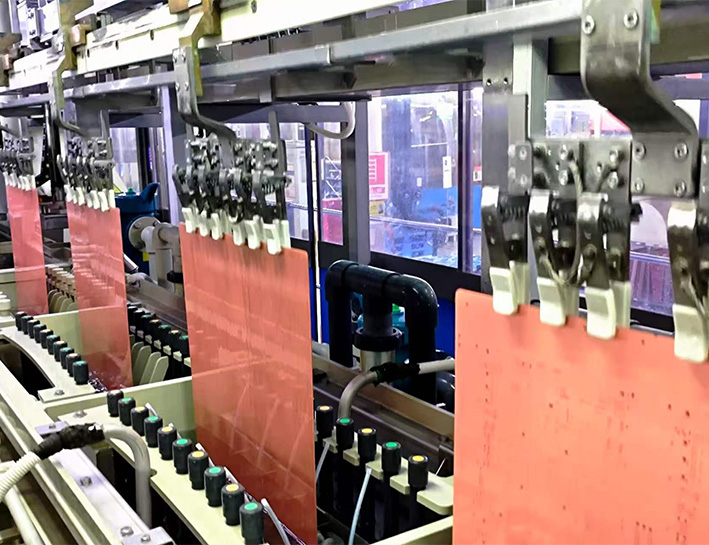
Patent Self-Tensioning Hanging System
Designed for ultra-thin substrates below 0.1mm, featuring a “dynamic stretching” architecture that eliminates frame edge effects, achieving thickness variation COV < 5%.
Detail Section 02
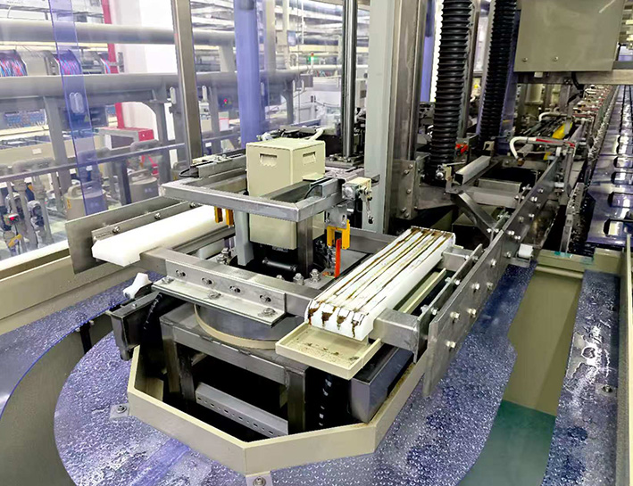
Zero Contact Physical Protection
Contactless conductive transmission logic throughout the entire process, isolating any friction mechanisms, ensuring zero scratches on circuits below 20μm.
Detail Section 03
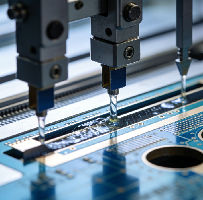
mSAP High Yield Flow Field Control
The chemical flow channel, combined with a gas-liquid separator, achieves a bubble-free effect in deep blind vias, improving the through-put yield of any-layer HDI.
Detail Section 04
EPC Full-Process Delivery & Commissioning
JADA’s hands-on team provides turnkey services ranging from hanger design to chemical compatibility verification, offering in-depth support for the Rohm and Haas EVF4 system.